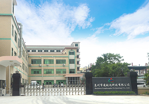
Time:2022-07-16 Views:994
With the continuous increase in the production ratio of flexible PCBs and the application and promotion of rigid-flex PCBs, it is more common to add softness, rigidity or rigid-flexibility to PCBs and say it is a few-layer FPC. Generally, FPC made of soft insulating substrate is called flexible FPC or flexible FPC, and rigid-flex composite PCB is called rigid-flex PCB. It meets the needs of today's electronic products in the direction of high density and reliability, small scale and light weight, and also meets the strict economic requirements and the needs of market and technological competition.
Overseas, flexible PCBs have been widely used in the early 1960s. In my country, it only started to produce applications in the 1960s. In recent years, with the global economic integration and the opening up of the market, the introduction of technology has continued to increase its application, and some small and medium-sized rigid FPC factories deem it appropriate to use soft and hard work techniques to take advantage of the existing The facility implements improvements to tooling tools and processes, transforming the production of flexible PCBs and meeting the ever-increasing demand for flexible PCBs. In order to further understand the PCB, here is a research and discussion introduction to the flexible PCB process.
1. Classification of flexible PCBs and their advantages and disadvantages
1. Classification of flexible PCBs
Flexible PCBs are generally classified as follows according to the number of layers and structures of conductors:
1.1 Single-sided flexible PCB
Single-sided flexible PCB has only one layer of conductor, and the outer surface can have a covering layer or no covering layer. The insulating base material used varies with the application of the product. Commonly used insulating materials are polyester, polyimide, polytetrafluoroethylene, flexible epoxy oxygen-glass cloth, etc.
Single-sided flexible PCB can be further divided into the following four categories:
1) One-sided joint signature without covering layer
The wire pattern of this type of flexible PCB is on the insulating substrate, and the wire surface has no covering layer. Same as general single-sided rigid FPC. This type of product is the cheapest one and is generally used in non-critical and background-focused applications. The interconnection is successfully achieved by soldering, fusion bonding or pressure bonding. It was commonly used in early telephones.
2) One-sided joint signature with covering layer
This type is comparable to the previous type, but according to customer requirements, there is an extra layer of covering layer on the surface of the wire. When covering, it is necessary to expose the pad, and it is simple to not cover the end area. If precision is required, the clearance hole method can be used as appropriate. It is one of the most widely used single-sided flexible PCBs, and is widely used in vehicle instruments and electronic spectrographs.
3) Double-sided joint signature without covering layer
This type of splicing pad interface can be attached on the front and back of the wire. To do this, a via hole is made in the insulating substrate at the pad, which can be punched, etched, or otherwise mechanically made at the desired location on the insulating substrate. It is used for mounting components and components on both sides and where soldering is required. There is no insulating substrate in the pad area of the via, and such pad areas are generally removed by chemical methods.

4) Double-sided joint signature with covering layer
This type is different from the previous type in that there is a covering layer on the outside. However, the cover layer has vias, which also allow termination on both sides and still maintain the cover layer. This type of flexible PCB is made of two layers of insulating material and one layer of metal conductors. It is used in the occasions where the cover layer and the surrounding devices are required to be insulated from each other, and they must be insulated from each other, and the ends need to be connected on both the front and the back.
1.2 Double-sided flexible PCB
Double-sided flexible PCB with two layers of conductors. The application and advantages of this type of double-sided flexible PCB are the same as those of single-sided flexible PCB. Its main advantage is to increase the wiring density per unit plane or surface of the object. It can be divided into with and without metallized holes and with or without cover layer: a without metallized holes and without cover layer; b without metallized holes and with cover layer; c with metallized holes and without cover layer ;d with metallized holes, with a masking layer. Double-sided flexible PCBs with no cover layer are less used.
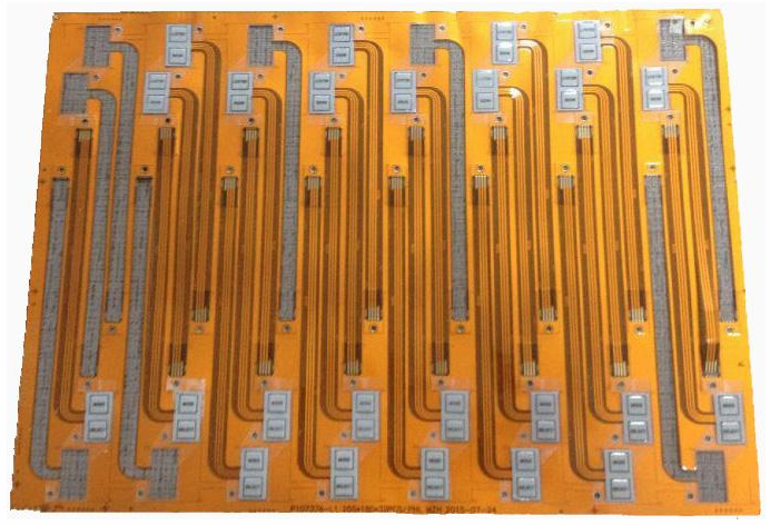
1.3-layer flexible PCB
Flexible multi-layer PCBs are like rigid multi-layer PCBs. Multi-layer lamination technology is used as appropriate to make multi-layer FPC flexible circuit boards. The simplest multi-layer flexible PCB is a three-layer flexible PCB formed by covering two layers of copper shielding layers on both sides of a single-sided PCB. The electrical properties of this three-layer flexible PCB are better than those of coaxial wires or shielded wires. The most commonly used multi-layer flexible PCB structure is a four-layer structure, and the interlayer interconnection is successfully achieved with metallized holes.
The advantage of multi-layer flexible PCB is that the substrate film is light in weight and has good electrical special properties, such as low dielectric constant. The multi-layer flexible PCB board made of polyimide film is about 1/3 lighter than the rigid epoxy glass cloth multi-layer PCB board, but it misses the single-sided and double-sided flexible PCB Good flexibility, most of these products do not require flexibility.
Multilayer flexible PCB can be further divided into the following types:
1) A multi-layer PCB is formed on a flexible insulating substrate, and the finished product is specified to be flexible: this structure generally bonds the two sides of many single-sided or double-sided microstrip flexible PCBs together, but that The inner core part is not bonded together, so it is highly flexible. In order to have the desired electrical special properties, such as special properties impedance performance matching with the rigid PCB to which it is interconnected, each circuit layer of the multilayer flexible PCB device must be pre-set signal lines on the ground plane. For a high degree of flexibility, a thin, conformable coating, such as polyimide, can be used on the conductor layer instead of a thicker laminated cover layer. The metallized holes enable the z-plane between the flexible wiring layers to successfully achieve the desired interconnection. This multi-layer flexible PCB is most suitable for use in designs that require flexibility, high reliability and high density.
2) A multi-layer PCB is formed on a flexible insulating substrate, and the finished product can be flexed at the end: this type of multi-layer flexible PCB is made of a flexible insulating material, such as a polyimide film, which is suppressed into a multi-layer board. The inherent flexibility is missed after lamination. This type of flexible PCB is considered appropriate when it is pre-set that the special properties of film insulation, such as low dielectric constant, thickness average medium, light weight, and continuous processing, are required to be utilized to an upper limit. For example, a multilayer PCB made with polyimide film insulation is about one-third lighter than a rigid epoxy-glass cloth PCB.
3) Multi-layer PCB is formed on a flexible insulating substrate, and the finished product must be formable, not continuously flexed: This type of multilayer flexible PCB is made of soft insulating material. Although it is made of soft materials, it is limited by electrical presets, such as requiring a thick conductor for the required conductor resistance, or requiring a thick conductor between the signal layer and the ground layer for the required impedance or capacitance. Thick insulating isolation, because of this, is formed when the finished product is applied. The term "formable" is defined as a multi-layer flexible PCB device that has experience in forming the required form and is no longer capable of flexing during application. Used in wiring inside avionics facility units. At this time, the stripline or three-dimensional space preset conductors are required to have low resistance, minimal capacitive coupling or circuit noise, and a flat and smooth 90° flex at the interconnect end. The multi-layer flexible PCB made of polyimide film material successfully realized the work of this wiring. Since the polyimide film is resistant to high temperature, flexible, and has special electrical and mechanical properties in general. In order to successfully realize the full interconnection of this device profile, the traces in there can be further divided into multiple multi-layer flexible circuit devices and assembled with adhesive tapes to form a printed circuit bundle.
1.4 Rigid-Flexible Multilayer PCB
This type is generally on one or two rigid PCBs, which contain the flexible PCBs necessary to form a group. Flexible PCB layers are laminated within rigid multilayer PCBs, either for special electrical requirements or to extend beyond rigid circuits, with the simplest surface circuit assembly experience. Such products are widely used in electronic devices where compression weight and size are the key, and high reliability, high density assembly and good electrical special properties are required.
Rigid-flex multi-layer PCB can also suppress the end bonding of many single-sided or double-sided flexible PCBs together into a rigid part, while the half-middle waist is not glued into a soft part, and the Z-side of the rigid part is used. Metallized via interconnects. Flexible circuits can be laminated into rigid multilayer boards. This type of PCB is increasingly used in applications that require ultra-high packaging density, good electrical properties, high reliability and strict size limits.
There is already a range of hybrid multilayer flexible PCB devices ready for use in military avionics, where weight and size are critical. In order to meet the specified weight and size limits, the packing density inside must be extremely high. In addition to the high density of the circuit, in order to minimize crosstalk and noise, all signal transmission lines must be shielded. If shielded clutch wires are to be used, it is virtually impossible to package them economically into a system. Thus, mixed multi-layers are used
Flexible PCB to successfully realize its interconnection. This device contains shielded signal lines in a flat stripline flexible PCB, which is an integral part of a rigid PCB. In relatively high-level operating situations, after fabrication, the PCB forms a 90° S-shaped buckling, thus providing the z-simplest path for surface interconnection, and under the effect of the simplest surface-oscillating stress in x, y, and z , which relieves stress-strain on solder joints.
2. Strengths Rigid area scope Rigid area scope
2.1 Flexibility
A significant advantage of using flexible FPC is that it can be more easily routed and connected in three-dimensional space, and can also be rolled or folded for use. As long as it is curled within the allowable radius of curvature, it can withstand thousands to tens of thousands of uses without damage.
2.2 Reduce the size
In the assembly and connection of components, compared with the use of conductor cables, the conductor profile of the flexible PCB is thin and flat, which reduces the size of the conductors, and can be formed along the casing, making the structure of the device more compact and reasonable, reducing the Installed even size. Compared with rigid PCB, the space can be saved by 60~90%.
2.3 Reduce weight
In the same size, the weight of flexible PCB and wire and cable can be reduced by about 70% under the same current carrying capacity, and compared with rigid PCB, the weight can be reduced by about 90%.
2.4 The exact sameness of the installation
It is connected with flexible PCB, which eliminates the error when wiring with wire and cable. As long as the processing drawings are corrected, all the winding circuits produced in the future are the same. There will be no misconnection when installing the connection cable.
2.5 increases reliability
When it is considered appropriate to use a flexible PCB for connection, because the wiring can be made on the three simplest planes of X, Y, and Z, the transfer interconnection is degraded, the reliability of the whole system is increased, and the detection of faults can be improved. Provides convenience.
2.6 Preset controllability of electrical parameters
According to application requirements, designers can control capacitance, inductance, special characteristic impedance, delay and attenuation, etc. when implementing flexible PCB design. Can be preset to have the special properties of a conveyor line. Since these parameters are related to wire width, thickness, spacing, insulation thickness, dielectric constant, damage tangent, etc., this is not easy to do when using wire and cable as deemed appropriate.
2.7 The end can be soldered in groups
Like rigid PCBs, flexible PCBs have terminal pads, which can eliminate wire stripping and tinning, thus saving costs. Terminal pads are connected to elements, components, and plugs, and dip or wave soldering can be used to replace manual soldering of each wire.
2.8 The use of materials can be selected
Flexible PCB can be made of different base materials according to different application requirements. For example, in assembly applications requiring low cost, polyester film can be used. In demanding applications where good performance is required, polyimide films can be used.
2.9 Low cost
The use of flexible PCB assembly can reduce the total cost. This is because:
1) Because the various parameters of the wires of the flexible PCB are exactly the same; the implementation of group termination eliminates the incorrect and reworked cable guides that often occur, and the modification of the flexible PCB is more convenient.
2) The application of flexible PCB simplifies the structural design, it can be directly pasted to the component, reducing the clip and its fixing parts.
3) For conductors that require shielding, the price of using flexible PCB is lower.
2.10 Continuity of processing
Because the flexible foil clad board can be continuously supplied in rolls, because this can successfully realize the continuous production of FPC closed doors. This also helps reduce costs.
3. Lack of
3.1 One-off initial cost is high
Because flexible PCBs are pre-configured and fabricated for specific applications, the cost of starting circuit pre-sets, wiring, and photographic negatives is high. In addition to the use of flexible PCBs for special needs, it is best not to use them when they are generally used in small quantities.
3.2 It is difficult to change and patch the flexible PCB
Once the flexible PCB is made, it must be changed from the base map or the woven light painting process, because this is not easy to change. Its surface is covered with a layer of protective film, which must be removed before patching and restored after patching, which is a relatively difficult office.
3.3 Size is limited
Flexible PCBs are generally made by batch process under uncommon working conditions. Because this is limited by the size of the production facility, it cannot be made very long and wide.
3.4 Improper operation and easy damage
The inappropriate operation of the person in charge of the installation can easily lead to the destruction of the flexible circuit, and its soldering and rework need to be operated by the person in charge of the training.


+86 18825066881 (Mr. Liu)

sales@lhdxlb.com

For inquiries about our products or price list, please leave us and we will contact you within 24 hours.