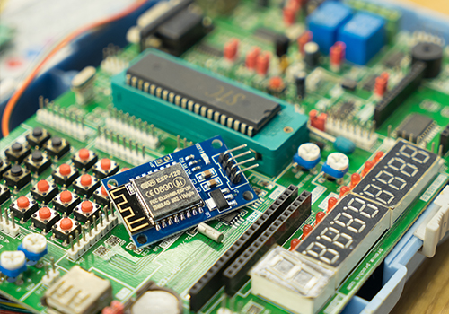
Time:2022-07-08 Views:994
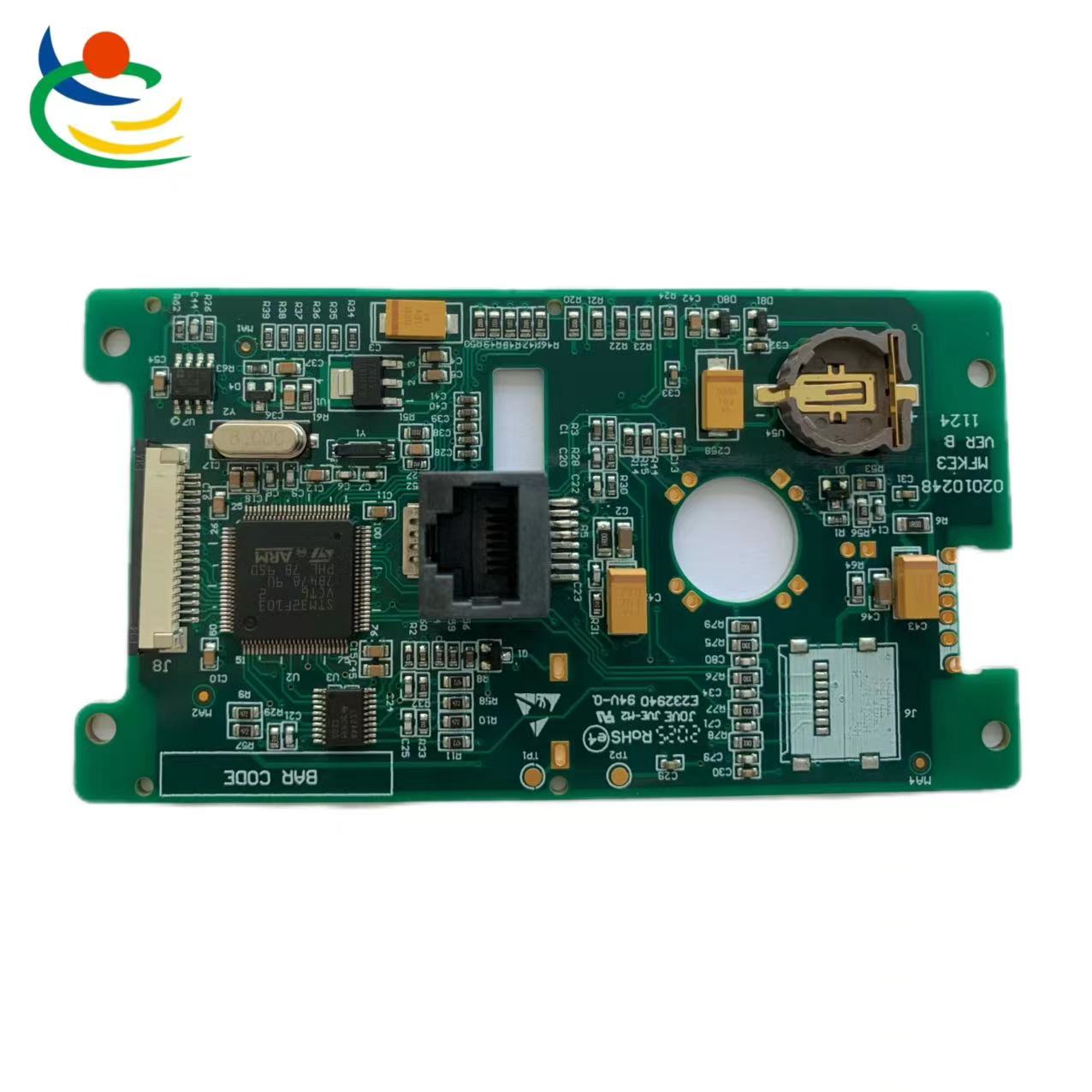
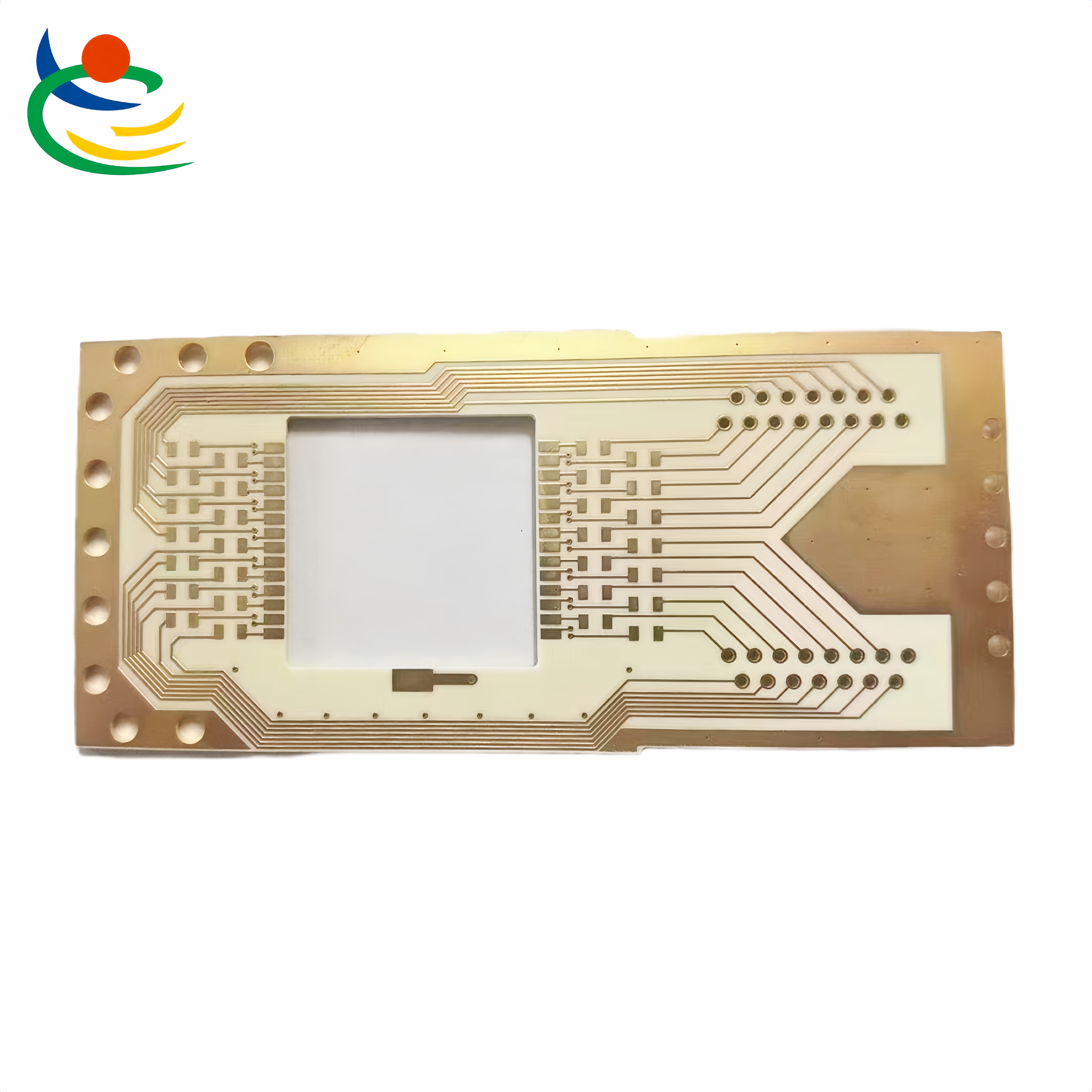
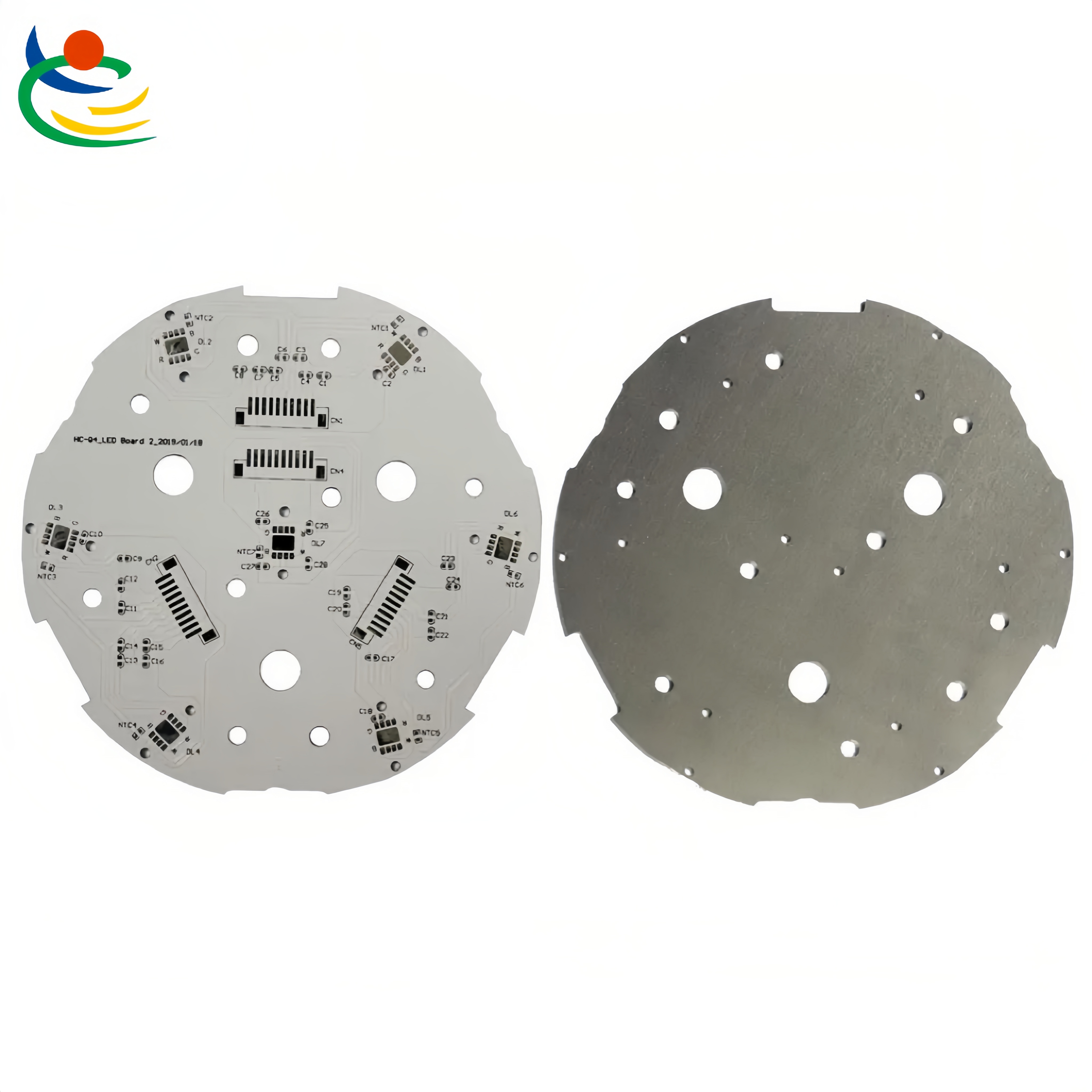
Shenzhen Linghangda Circuit Board Technology Co., Ltd. is a high-tech enterprise specializing in the production and sales of single-sided and multi-layer circuit boards. The company has a professional CAD, CAM circuit board design, copy board and after-sales service team, providing a full range of one-stop services from circuit board design to manufacturing for well-known enterprises at home and abroad.
PCB circuit board design needs to provide information:
1. Schematic diagram: a complete electronic document format that can generate the correct netlist;
2. Mechanical size: Provide the specific position and direction identification of the positioning device, as well as the identification of the specific height limit position area;
3. BOM list: mainly to determine and check the specified package information of the device on the schematic diagram;
4. Wiring Guide: Description of specific requirements for special signals, as well as design requirements for impedance, stacking, etc.
The basic design process of PCB circuit board design is as follows:
Preliminary preparation -> PCB structure design -> PCB layout -> routing -> routing optimization and silk screen -> network and DRC inspection and structural inspection -> pattern making.
1. Preliminary preparation
1. This includes preparing component libraries and schematics. "If you want to do a good job, you must first sharpen your tools." To make a good board, in addition to designing the principles, you must also draw well. Before proceeding with the PCB design, first prepare the component library of the schematic SCH and the component library of the PCB (this is the first step - very important). The component library can use the library that comes with Protel, but it is generally difficult to find a suitable one. It is best to make your own component library according to the standard size data of the selected device.
In principle, make the component library of PCB first, and then make the component library of SCH. The PCB component library has high requirements, which directly affects the installation of the board; the SCH component library requirements are relatively loose, as long as you pay attention to defining the pin attributes and the corresponding relationship with the PCB components.
PS: Note the hidden pins in the standard library. After that is the design of the schematic diagram, and then ready to start the PCB design.
2. When making the library of the schematic diagram, pay attention to whether the pins are connected/output to the PCB board and check the made library.
2. PCB structure design
In this step, according to the determined plane size of the circuit board and various mechanical positioning, draw the PCB surface in the PCB design environment, and place the required connectors, buttons/switches, digital tubes, indicator lights, input and output according to the positioning requirements. , screw holes, assembly holes, etc., and fully consider and determine the wiring area and non-wiring area (such as how much area around the screw hole belongs to the non-wiring area).
(Special attention should be paid to the actual size of the components (occupied area and height), the relative position-spatial size between the components, and the surface on which the components are placed to ensure the electrical properties of the circuit board when placing components. At the same time, the performance and the feasibility and convenience of production and installation should be properly modified on the premise of ensuring that the above principles can be reflected to make them neat and beautiful. For example, the same devices should be placed neatly and in the same direction. "patched").
3. PCB layout
1. Make sure the schematic is correct before layout - this is important! -----Very important!
After the schematic diagram is drawn, check the items: power network, ground network, etc.
2. When laying out, pay attention to the surface on which the device is placed (especially the plug-in, etc.) and the placement method of the device (in-line or vertical) to ensure the feasibility and convenience of installation.
3. To put it bluntly, the layout is to put devices on the board. At this time, if the preparations mentioned above are done, you can generate a netlist (Design->CreateNetlist) on the schematic diagram, and then import the netlist (Design->LoadNets) on the PCB diagram. You can see that the devices are all piled up, and there are flying wires between the pins to indicate the connection, and then you can lay out the devices.
The general layout is carried out according to the following principles:
The surface on which the device is placed should be determined during layout: Generally speaking, the patch should be placed on the same side, and the plug-in depends on the specific situation.
① According to the reasonable division of electrical performance, it is generally divided into: digital circuit area (that is, afraid of interference and interference), analog circuit area (afraid of interference), and power drive area (interference source);
②The circuit that completes the same function should be placed as close as possible, and each component should be adjusted to ensure the most concise connection; at the same time, the relative position of each functional block should be adjusted to make the connection between the functional blocks the most concise;
③ For components with large mass, the installation position and installation strength should be considered; heating elements should be placed separately from temperature-sensitive components, and thermal convection measures should be considered if necessary;
④ The I/O drive device should be as close as possible to the edge of the printed circuit board and the lead-out connector;
⑤ The clock generator (such as: crystal oscillator or clock oscillator) should be as close as possible to the device that uses the clock;
⑥ The layout requirements should be balanced, dense and orderly, and should not be top-heavy or heavy.
Fourth, wiring
Routing is the most important process in the entire PCB design. This will directly affect the performance of the PCB board. In the process of PCB design, there are generally three divisions of wiring: the first is routing, which is the most basic requirement for PCB design. If the lines are not laid out, and there are flying wires everywhere, it will be an unqualified board, and it can be said that it has not yet started. The second is the satisfaction of electrical performance. This is a measure of whether a printed circuit board is qualified. This is after the layout, carefully adjusting the wiring so that it can achieve the best electrical performance, followed by aesthetics. If your wiring is connected, there is nothing to affect the performance of the electrical appliance, but at first glance, it is messy and colorful, and then no matter how good your electrical performance is, it is still a piece of garbage in the eyes of others. This brings great inconvenience to testing and maintenance. The wiring should be neat and uniform, and it should not be criss-crossed without any rules. These must be realized under the condition of ensuring the performance of the electrical appliance and meeting other individual requirements, otherwise it will be abandoned.
The wiring is mainly carried out according to the following principles:
①In general, the power line and ground line should be wired first to ensure the electrical performance of the circuit board. Within the scope of conditions, try to widen the width of the power supply and the ground wire. It is better that the ground wire is wider than the power supply wire. , the thinnest width can reach 0.05~0.07mm, and the power line is generally 1.2~2.5mm. For the PCB of the digital circuit, a wide ground wire can be used to form a loop, that is, a ground net can be used (the ground of the analog circuit cannot be used in this way. );
②Wire the lines with strict requirements (such as high-frequency lines) in advance. The edges of the input end and the output end should be avoided to be parallel to each other to avoid reflection interference. If necessary, the ground wire should be isolated, and the wiring of two adjacent layers should be mutually Vertical and parallel are prone to parasitic coupling;
③The oscillator shell is grounded, and the clock line should be as short as possible, and it should not be drawn everywhere. Under the clock oscillation circuit, the special high-speed logic circuit part should increase the area of the ground, and other signal lines should not be used to make the surrounding electric field approach zero;
4. Use 45° folded line wiring as much as possible, and 90° folded line cannot be used to reduce the radiation of high-frequency signals; (double arcs should be used for lines with high requirements);
⑤ Do not form a loop in any signal line. If it is unavoidable, the loop should be as small as possible; the vias of the signal line should be as few as possible;
⑥ The key lines should be as short and thick as possible, and protective ground should be added on both sides;
⑦ When transmitting sensitive signals and noise field signals through flat cables, use the method of "ground wire-signal-ground wire";
⑧ Test points should be reserved for key signals to facilitate debugging, production and maintenance testing;
⑨ After the schematic diagram wiring is completed, the wiring should be optimized; at the same time, after the preliminary network inspection and DRC inspection are correct, the unwiring area is filled with ground wires, and a large area of copper layer is used as the ground wire. The places that are not used are connected to the ground as a ground wire. Or make a multi-layer board, power supply, ground wire each occupy one layer.
5. Add teardrops
The teardrop is the excessive connection between the pad and the wire or the wire and the guide hole. The purpose of setting the teardrop is to avoid the contact point between the wire and the pad or the wire and the guide hole when the circuit board is impacted by a huge external force. Disconnecting, additionally, setting teardrops can also make the PCB board appear more aesthetically pleasing.
In circuit board design, in order to make the pads stronger and prevent the disconnection between the pads and the wires during mechanical board making, a transition area is often arranged with a copper film between the pads and the wires, which is shaped like a teardrop, so it is often called Make up teardrops ( Teardrops ).
Sixth, check the first item, look at the Keepout layer, top layer, bottom layer topoverlay, bottomoverlay in turn.
Seven, electrical rules check: vias (0 vias - very incredible; 0.8 dividing line), whether there is a disconnected netlist, minimum spacing (10mil), short circuit (analyze each parameter one by one)
8. Inspection of power cord and ground wire - interference. (The filter capacitor should be close to the chip)
9. After the PCB is completed, reload the net mark to check whether the netlist has been modified - it works.
10. After the PCB is completed, check the lines of the core components to ensure that they are accurate.
Well, the above is the basic process of PCB circuit board design. Friends who have PCB design needs are welcome to consult us!


+86 18825066881 (Mr. Liu)

sales@lhdxlb.com

For inquiries about our products or price list, please leave us and we will contact you within 24 hours.