Time:2022-07-09 Views:869
Many friends are interested in the PCB design process. Next, Shenzhen Honglijie will introduce the design process from schematic diagram to PCB.
1. Design process from schematic diagram to PCB
Create component parameters -> input principle netlist -> design parameter settings -> manual layout -> manual routing -> verify design -> review -> CAM output.
2. Parameter setting
The spacing between adjacent conductors must meet electrical safety requirements, and for ease of operation and production, the spacing should be as wide as possible. The minimum spacing should be at least suitable for the withstand voltage. When the wiring density is low, the spacing of the signal lines can be appropriately increased. For the signal lines with high and low level differences, the distance should be as short as possible and the spacing should be increased. Set the trace spacing to 8mil. The distance from the edge of the inner hole of the pad to the edge of the printed board should be greater than 1mm, so as to avoid the defect of the pad during processing. When the traces connected to the pads are thin, the connection between the pads and the traces should be designed in a water drop shape. The advantage of this is that the pads are not easy to peel, but the traces and the pads are not easily disconnected.
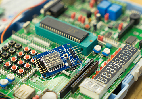
3. Component layout
Practice has proved that even if the circuit schematic design is correct, the PCB design is not properly designed, which will adversely affect the reliability of electronic equipment. For example, if the two thin parallel lines of the printed board are very close, the delay of the signal waveform will be formed, and the reflection noise will be formed at the end of the transmission line; The performance is degraded, so care should be taken to use the correct method when designing the printed circuit board.
Each switching power supply has four current loops:
(1). Power switch AC circuit
(2). Output rectifier AC circuit
(3). Input signal source current loop
(4). Output load current loop
The input loop charges the input capacitor with an approximate DC current, and the filter capacitor mainly acts as a broadband energy storage; similarly, the output filter capacitor is also used to store the high-frequency energy from the output rectifier, while eliminating the DC energy of the output load loop . Therefore, the terminals of the input and output filter capacitors are very important, and the input and output current loops should be connected to the power supply only from the terminals of the filter capacitors; if the connection between the input/output loop and the power switch/rectifier loop cannot be The terminals are directly connected, and the AC energy will be radiated into the environment by the input or output filter capacitors. The AC loop of the power switch and the AC loop of the rectifier contain high-amplitude trapezoidal currents. These currents have high harmonic content, the frequency is much higher than the switching fundamental frequency, and the peak amplitude can be as high as 5 times the amplitude of the continuous input/output DC current. The transition time is usually about 50ns. These two loops are most likely to generate electromagnetic interference, so these AC loops must be laid out before other traces in the power supply are routed. The three main components of each loop, filter capacitors, power switches or rectifiers, inductors or transformers, should be connected to each other. Place them next to each other, adjusting the position of the components so that the current paths between them are as short as possible.
The best way to establish a switching power supply layout is similar to its electrical design, and the best design flow is as follows:
1. Place the transformer
2. Design the power switch current loop
3. Design the output rectifier current loop
4. Control circuit connected to AC power circuit
Design the input current source loop and input filter Design the output load loop and output filter According to the functional unit of the circuit, when laying out all the components of the circuit, the following principles should be followed:
(1) First, consider the size of the PCB. When the PCB size is too large, the printed lines will be long, the impedance will increase, the anti-noise capability will decrease, and the cost will also increase; if the PCB size is too small, the heat dissipation will be poor, and the adjacent lines will be easily interfered. The best shape of the circuit board is a rectangle with an aspect ratio of 3:2 or 4:3. The components located on the edge of the circuit board are generally not less than 2mm away from the edge of the circuit board.
(2) When placing the device, consider the subsequent soldering, not too dense.
(3) Centering on the core components of each functional circuit, make layout around it. Components should be evenly, neatly and compactly arranged on the PCB, minimize and shorten the leads and connections between components, and place the decoupling capacitor as close to the VCC of the device as possible.
(4) For circuits operating at high frequencies, the distribution parameters between components should be considered. In general circuits, the components should be arranged in parallel as much as possible. In this way, it is not only beautiful, but also easy to install and weld, and easy to mass produce.
(5) Arrange the positions of each functional circuit unit according to the circuit flow, so that the layout is convenient for signal circulation, and the signals keep the same direction as possible.
(6) The primary principle of layout is to ensure the routing rate of wiring, pay attention to the connection of flying wires when moving devices, and put devices with a connection relationship together.
(7) Minimize the loop area as much as possible to suppress the radiation interference of the switching power supply.
4. Wiring
The switching power supply contains high-frequency signals, and any printed wire on the PCB can function as an antenna. The length and width of the printed wire will affect its impedance and inductance, thereby affecting the frequency response. Even traces passing through DC signals can couple to RF signals from adjacent traces and cause circuit problems (or even radiate interfering signals again). Therefore, all traces that carry AC current should be designed to be as short and wide as possible, which means that all components connected to the traces and to other power lines must be placed close together. The length of the trace is proportional to the inductance and impedance it exhibits, while the width is inversely proportional to the inductance and impedance of the trace. The length reflects the wavelength to which the trace responds. The longer the length, the lower the frequency at which the trace can transmit and receive electromagnetic waves, and the more RF energy it can radiate. According to the size of the printed circuit board current, try to increase the width of the power line to reduce the loop resistance. At the same time, make the direction of the power line and the ground line consistent with the direction of the current, which will help to enhance the anti-noise ability. Grounding is the bottom branch of the four current loops of the switching power supply. It plays an important role as the common reference point of the circuit, and it is an important method to control interference. Therefore, the placement of the ground wire should be carefully considered in the layout. Mixing various grounds will cause unstable power supply operation.
The following points should be paid attention to in the ground wire design:
1. Correctly select single-point grounding Usually, the common terminal of the filter capacitor should be the only connection point where other grounding points are coupled to the high-current AC ground. It should be connected to the grounding point of this level, mainly considering that the current returning to the ground from each part of the circuit changes, and the impedance of the actual line flowing through will cause the ground potential of each part of the circuit to change and introduce interference. In this switching power supply, its wiring and the inductance between the devices have little influence, and the circulating current formed by the grounding circuit has a greater influence on the interference, so one point grounding is adopted, that is, the ground wires of several devices in the power switch current loop are all Connected to the ground pin, the ground wires of several devices outputting the current loop of the rectifier are also connected to the ground pins of the corresponding filter capacitors, so that the power supply works more stably and is not easy to self-excite. When a single point cannot be achieved, the common ground Connect two diodes or a small resistor at the place. In fact, it can be connected to a relatively concentrated piece of copper foil.
2. Make the grounding wire as thick as possible. If the grounding wire is very thin, the grounding potential will change with the change of the current, which will make the timing signal level of the electronic equipment unstable and the anti-noise performance deteriorate. Use the short and wide printed wire as possible, and try to widen the width of the power and ground wires, preferably the ground wire is wider than the power wire, and their relationship is: ground wire > power wire > signal wire, if possible, the ground wire The width should be greater than 3mm, and a large-area copper layer can also be used as a ground wire. On the printed board, all places that are not used are connected to the ground as a ground wire.
(1) Wiring direction: From the welding surface, the arrangement of components should be as consistent as possible with the schematic diagram, and the wiring direction should preferably be consistent with the wiring direction of the circuit diagram, because various parameters are usually required on the welding surface during the production process. Therefore, it is convenient for inspection, debugging and maintenance in production (Note: refers to the premise of meeting the circuit performance and the requirements of the whole machine installation and panel layout).
(2) When designing the wiring diagram, the wiring should be turned as little as possible, the line width on the printing arc should not be abruptly changed, the corner of the wire should be ≥90 degrees, and the lines should be simple and clear.
(3). No cross circuit is allowed in the printed circuit. For lines that may cross, you can use "drilling" and "winding" to solve the problem. That is, let a lead "drill" through the gap under other resistors, capacitors, and triode pins, or "wrap" from one end of a lead that may cross. In special cases, the circuit is very complicated, and it is also allowed to simplify the design. Use wire jumpers to solve cross-circuit problems. Due to the single panel, the in-line components are located on the top surface, and the surface-mount devices are located on the bottom surface, so the in-line devices can overlap with the surface-mount devices during layout, but the overlapping of the pads should be avoided.
3. The input ground and output ground are low-voltage DC-DC in the local switching power supply. If the output voltage is to be fed back to the primary of the transformer, the circuits on both sides should have a common reference ground. connected together to form a common ground
5. Inspection
After the wiring design is completed, it is necessary to carefully check whether the wiring design conforms to the rules made by the designer, and at the same time, it is necessary to confirm whether the rules made meet the requirements of the printed board production process. Generally, check the lines and lines, lines and component pads, lines Whether the distance between the through hole, the component pad and the through hole, and the through hole and the through hole is reasonable, and whether it meets the production requirements. Whether the width of the power line and the ground line is appropriate, and whether there is any place in the PCB where the ground line can be widened. Note: Some errors can be ignored. For example, part of the Outline of some connectors is placed outside the board frame, and errors will occur when checking the spacing; in addition, after each modification of the traces and vias, the copper must be re-clad.
According to the "PCB Checklist", the content includes design rules, layer definition, line width, spacing, pads, and via settings. It is also necessary to review the rationality of device layout, power supply, ground network routing, and high-speed clock network. The wiring and shielding, placement and connection of decoupling capacitors, etc.
6. Design output
Notes on outputting lightpaint files:
a. The layers that need to be output are wiring layer (bottom layer), silk screen layer (including top layer silk screen, bottom layer silk screen), solder mask layer (bottom layer solder mask), drilling layer (bottom layer), in addition to generate drill file (NC Drill) )
b. When setting the Layer of the silk screen layer, do not select PART Type, select the top layer (bottom layer) and Outline, Text, Linec of the silk screen layer. When setting the Layer of each layer, select Board Outline, and when setting the Layer of the silk screen layer, Do not select PART Type, select Outline, Text, Line of the top layer (bottom layer) and silkscreen layer. d. When generating the drill file, use the default settings of PowerPCB without making any changes.


+86 18825066881 (Mr. Liu)

sales@lhdxlb.com

For inquiries about our products or price list, please leave us and we will contact you within 24 hours.