Time:2023-07-06 Views:591
Board constraints, including board size and shape, need to be considered when designing a printed circuit board. First, we need to confirm that there is enough space for the circuit. The size of the board is affected by many factors, such as the size and function of the final product. Along with With the advancement of technology and changes in consumer demand, electronic products are getting smaller and more versatile, which also greatly affects the PCB design. Therefore, it is very important to estimate the PCB size before starting the design. If there is not enough Space, we may need to use multi-layer or high-density interconnect (HDI) design to achieve the desired function. Regarding the shape, we generally design the PCB as a rectangle, but for some products with irregular shapes, the PCB used also needs to be designed Into a special shape, although it will increase the cost. At the same time, we need to consider the number of layers in the early stage of PCB design. Designing a PCB with more layers will increase the cost, but it allows us to design a PCB with more advanced functions.
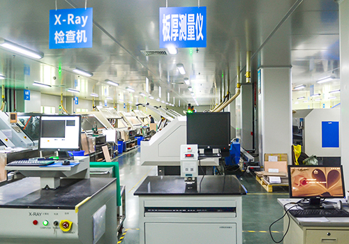
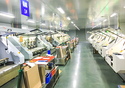
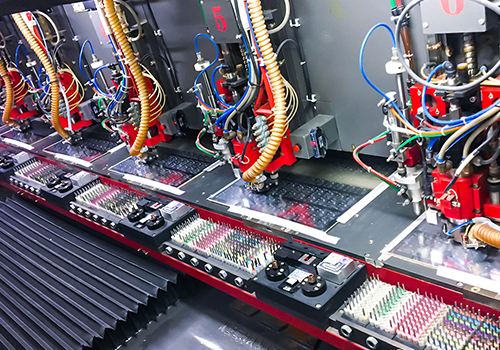
Before starting the PCB design, we need to consider the manufacturing process of the board, because different processes have different limits and constraints. Reference holes are needed to work with the manufacturing process on the board, and we should design components away from the PCB holes. Another On the one hand, we need to consider the raw materials and assembly methods used to make the PCB, for example, in some cases, they need to use both through-hole and surface mount components. In addition, communicate with manufacturers to ensure that they have the ability to produce the required circuit board type.
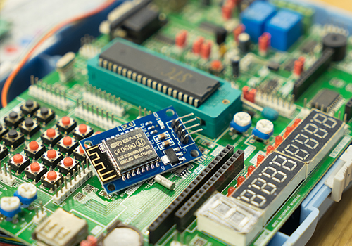
Before starting the PCB design, we should figure out the materials and components used by the board. The design may change according to different materials and components, and it will take some time to choose the right materials and components for the board. First, we need to confirm them Available, because some materials and components are hard to find in the market. At the same time, we should make sure to get the desired items within the budget. Finally, we also need to make sure that our design can maximize the advantages of these materials and components.
It refers to the process that involves the order in which we place components on the board. We recommend adding connectors and power circuits first, followed by precision circuits, critical circuits, and then other elements. During this process, we need to consider routing and Generation capability, noise susceptibility, routing priority, and power levels. If we place components in the wrong order it could cause circuit paths or component conflicts, and we need to go back to the drawing board stage.
The placement of components affects the performance of the PCB, and sometimes can make or break the final product. To help you get the desired results, we recommend not to place components too close together, which will bring many negative effects. First, it hinders the placement Automation of components, which leads to slow testing. If the components are placed too close together, the machine or the engineer has to be extra careful when placing and testing the board. Second, it will also take more time during the manufacturing phase, because the engineer has to be slow and Proceed with care. It is recommended to allow at least 100 mils of space between the component and the edge of the PCB.
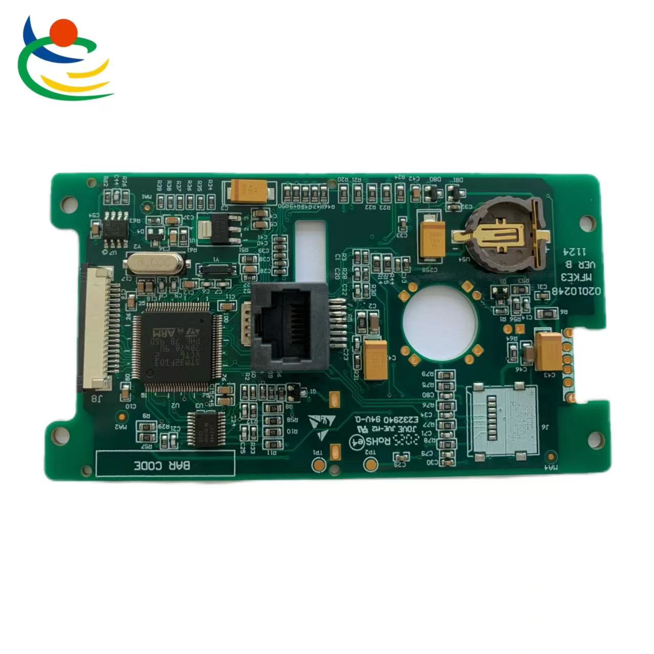
When we design a PCB, we should note that all electronic components on the board should face the same direction, which can help improve manufacturing and assembly efficiency by eliminating any confusion, especially during the soldering process.


+86 18825066881 (Mr. Liu)

sales@lhdxlb.com

For inquiries about our products or price list, please leave us and we will contact you within 24 hours.